英文
英文 中文
中文
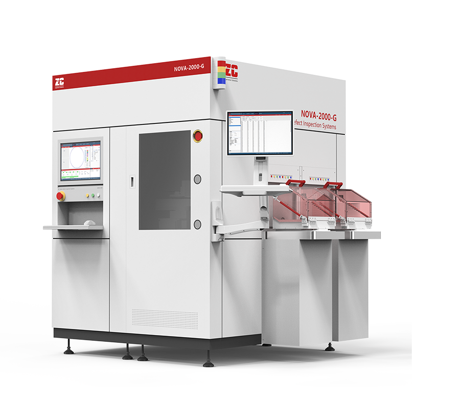
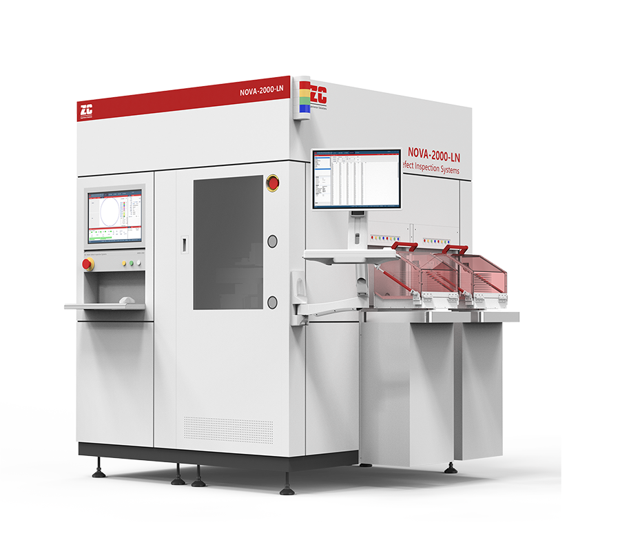
Inspection Equipment For Glass Wafers (NOVA-2000-G) is made for finding defects in transparent or semi-transparent wafer substrates, like glass and lithium niobate wafers. It can spot defects such as particles, scratches, pits, bumps, chipped edges, and cracks. This is important for controlling the quality of transparent wafers. The system uses different detection methods,like bright field and dark field. It gives reliable defect info for all kinds of problems. By using automatic defect detection and classification algorithms, it gets defect data such as the type, size, location, and stats. Then it makes a wafer defect report for users to judge the quality.
|
Inspection Equipment For Glass Wafers |
|
|
Model |
NOVA-2000-G |
|
Wafer Type |
Glass Wafer Substrates, Patterned Wafers |
|
Wafer Size |
4 inches, 6 inches, 8 inches, 12 inches (Compatible with adjacent sizes) |
|
Inspection Modes |
Bright-field, Dark-field, Differential Interference |
|
Resolution |
10μm-0.5μm |
|
Objectives |
1X, 2X, 5X, 10X, 20X, 50X |
|
Defect Types |
Scratches, pitting, particles, contamination, edge chipping, etc. |
|
Throughput |
≥12WPH (@8-inch wafer resolution 1μm) |
|
≥7WPH (@12-inch wafer resolution 1μm) |
|
|
Automation |
2 LoadPort |
Note: We can provide customized instruments of the same type and related testing solutions according to customer requirements.
-
Customized Clamping Method1
-
Backside Noise Suppression2
-
Real-time Automatic Focusing3
-
High Automation4
-
High Efficiency5
-
Intelligent Algorithm6
Read more

Inspection Equipment For SiC